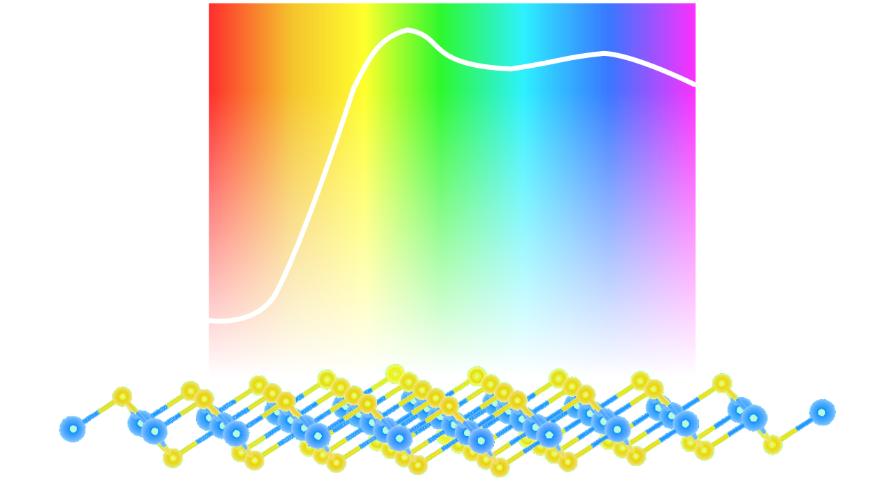
Certain layered crystals can change from semiconductors to metals just by altering their thickness, a unique trait of these materials that could lead to significant advancements in electronics and optics. One notable example of this is PtSe₂, which surprisingly remains mostly transparent in the infrared while still behaving like a metal in its thick form, a phenomenon that has confused scientists. Writing in the Physical Review Letters, Marin Tharrault et al. from the Nanooptics team of LPENS have resolved this apparent paradox by pinpointing the origin of light absorption in these materials. They identified the specific electronic transitions responsible for light absorption by carefully comparing precise measurements and simulations of the material’s electronic properties function of its thickness. Doing so, they ruled out the idea that phonon-assisted transitions were the main cause of light absorption, which had been the dominant explanation prior to this work. Their study also determines the number of layers required for the material to change its state, paving the way for innovative applications in technology.

Platinum diselenide optical absorption spectrum
More:
https://journals.aps.org/prl/abstract/10.1103/PhysRevLett.134.066901
Affiliation author:
Laboratoire de physique de L’École normale supérieure (LPENS, ENS Paris/CNRS/Sorbonne Université/Université de Paris)
Corresponding author: Emmanuel Baudin
Communication contact : L’équipe de communication


