


Equipement dedicated to the growth, the structuration and the characterisation of matter at the micro- and nano-scale are divised into 5 poles:
Lithography pole
Optical lithography
The optical lithography system is a Karl Süss MJB4 mask aligner, allowing to print a pattern in resist from a hard mask with a size up to 100x100mm, with writing resolution of 1μm.
It has the « split-field » option for the microscope, making the alignement easier for big surface samples.
Often used resists: AZ5214, S1805, SU8, PMGI and LOR-B.
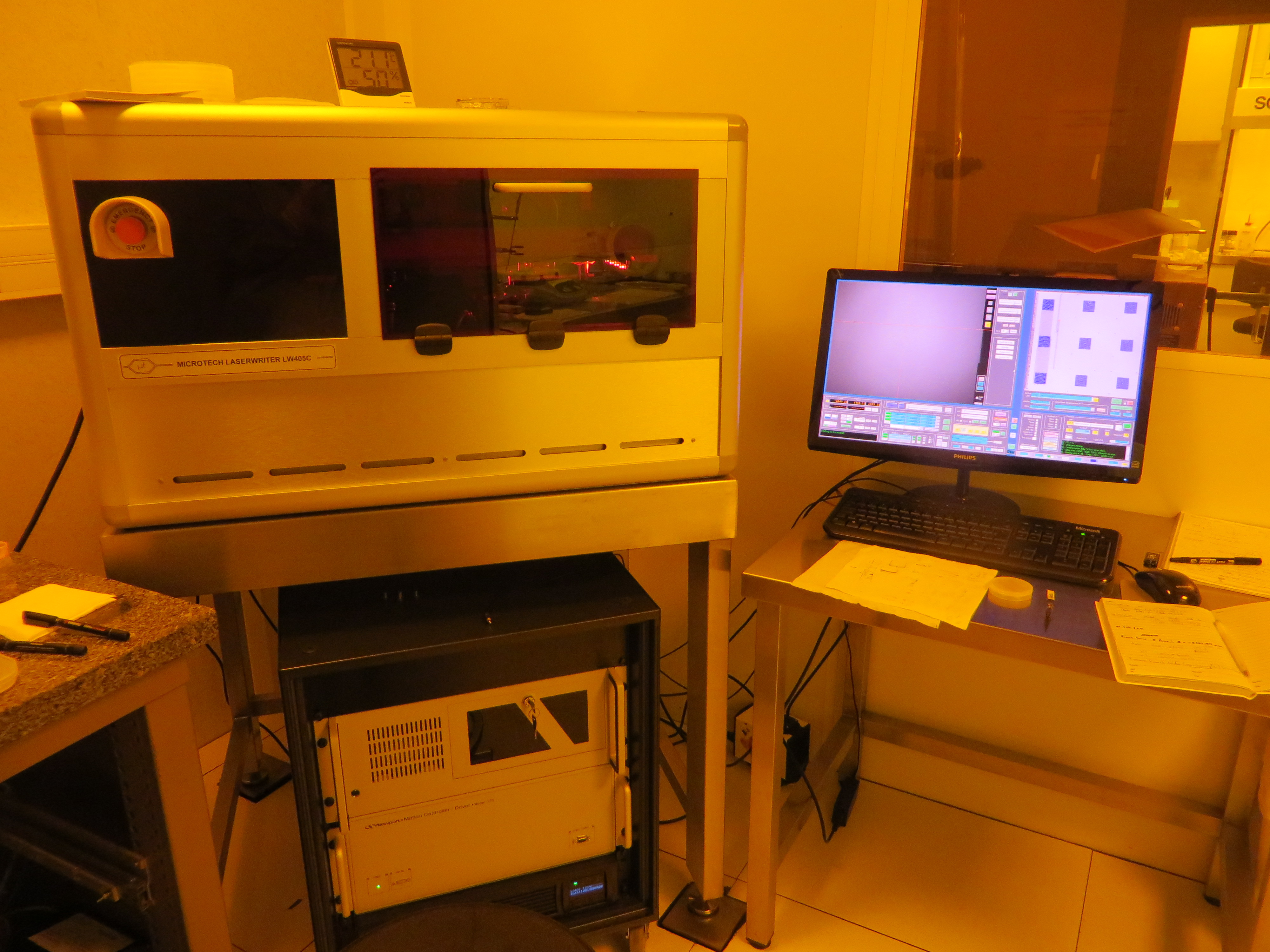
Laser lithography
The laser lithography is a LW405C Microtech system, equipped with a GaN laser at 405nm, allowing to print in resist all patterns with a 1μm resolution.
The writing field is 100 x 100 mm and a back-face alignement is possible with a position resolution of 5 µm.
Used resists: AZ5214 and S1805.
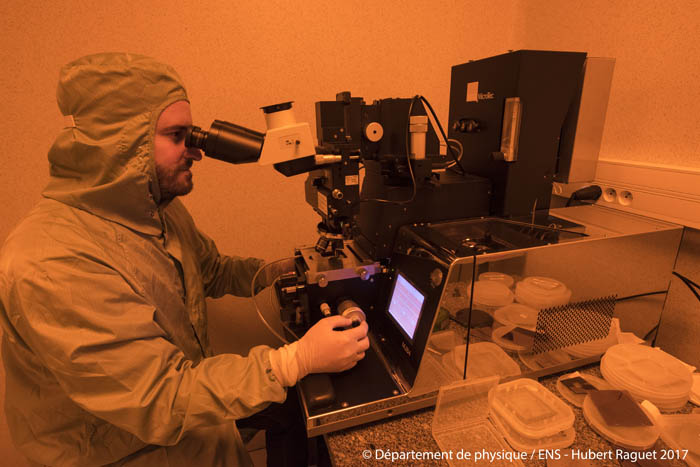
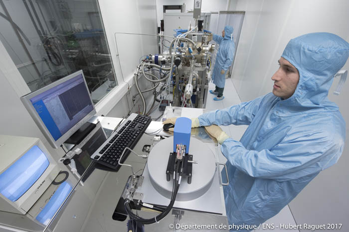
100keV electron lithography
The first electron lithography system is an ELS-BODEN 100 from Elionix. It has a writing resolution of 6nm in particular conditions. It allows samples from 0.5cm up to 8 pouces, and until eight 2″ wafers at the same time.
The BeamFox software is coupled with in order to correct proximity effets and make efficient fracturation.
- Often used resists: PMMA, HSQ, MaN, MAA, Cesar.
It also allows to make electron microscopy observations with a nm resolution, at high speed.

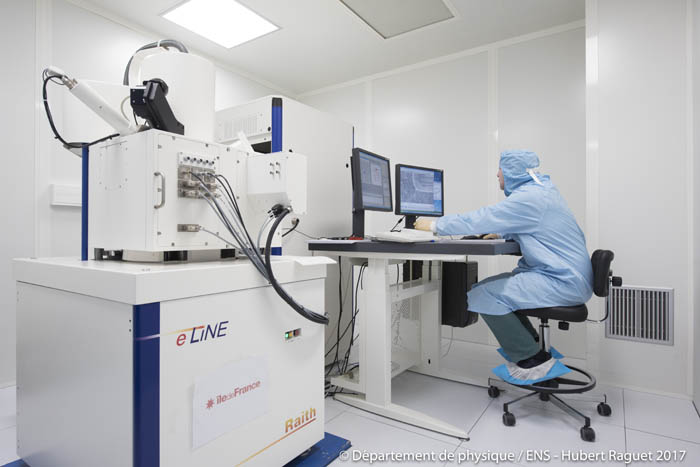
20keV electron lithography
The second electron lithography system is a Raith Eline SEM with a FEG-GEMINI column (0.5 – 30 kV) equipped with an interferometric stage of 100 X 100 mm. It has a writing resolution of 10nm in a 50 nm-thick PMMA.
- Installed options:
- Automatic Height Sensing, which correct focalisation losses during writing on big samples (> 2 “),
- FBMS (Fixed Beam Motor Stage) for a writing without field stitching;
- Often used resists: PMMA, HSQ, MaN, MAA.
With a FEG electron gun, two detectors (for in-column back-scattered electrons and for secondary electrons), it also allows to make electron imaging observations down the nm, including with a tilt.
Transfert pole
Plasma etching
The layer etching is made by a fluorinated reactive ion etching (RIE) in a 200R Corial system. Sample size up to 200 mm. The system has the option of end point detection by laser interferometry.
Available gas: Ar, O2, SF6 and CHF4.
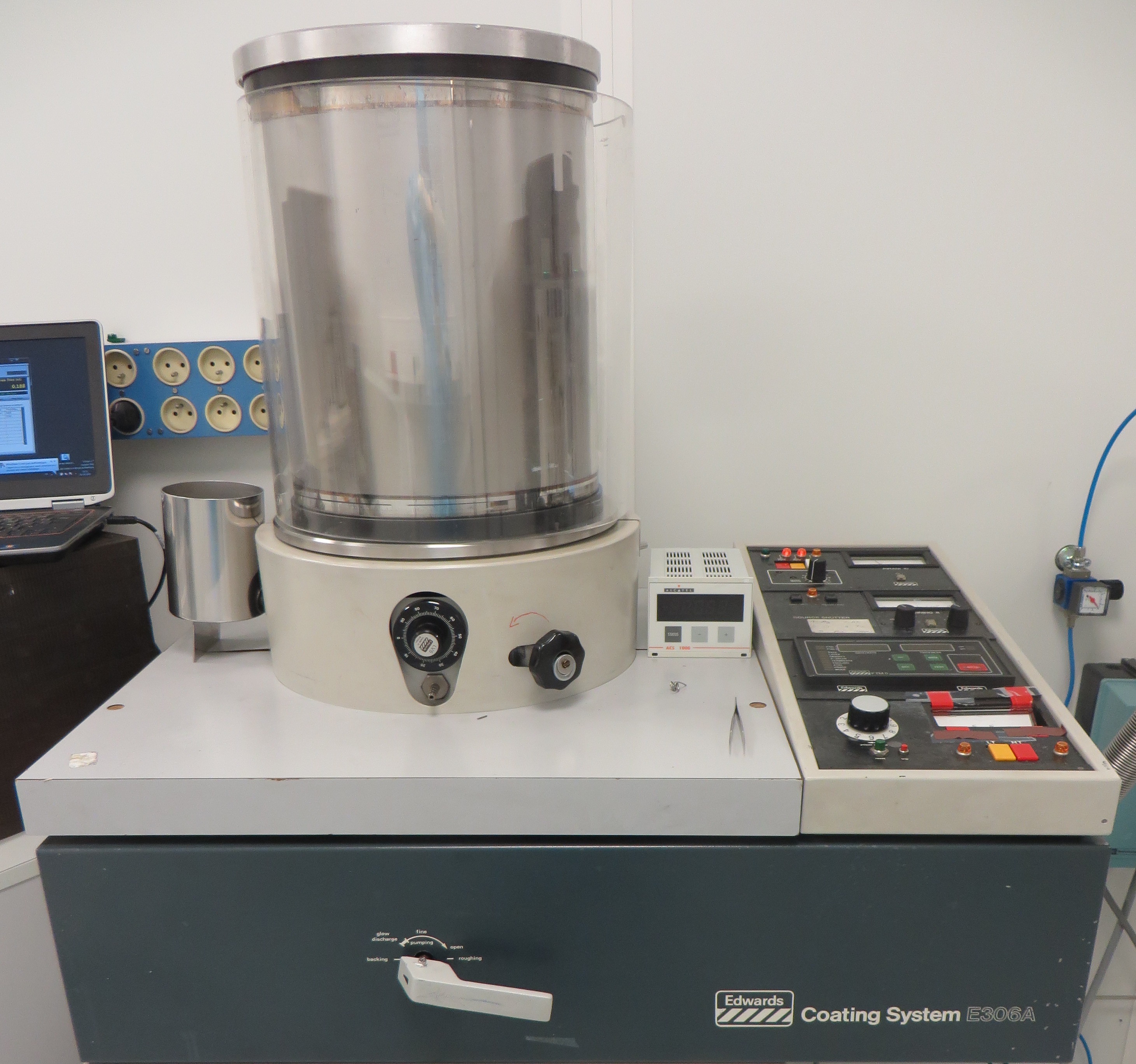
Joule effect evaporation
The Joule effect evaporator is an Edwards system with 4 crucibles, under high vacuum.
Materials: Cr, Au, Al, Ag and Ni. + O2 for oxydation.
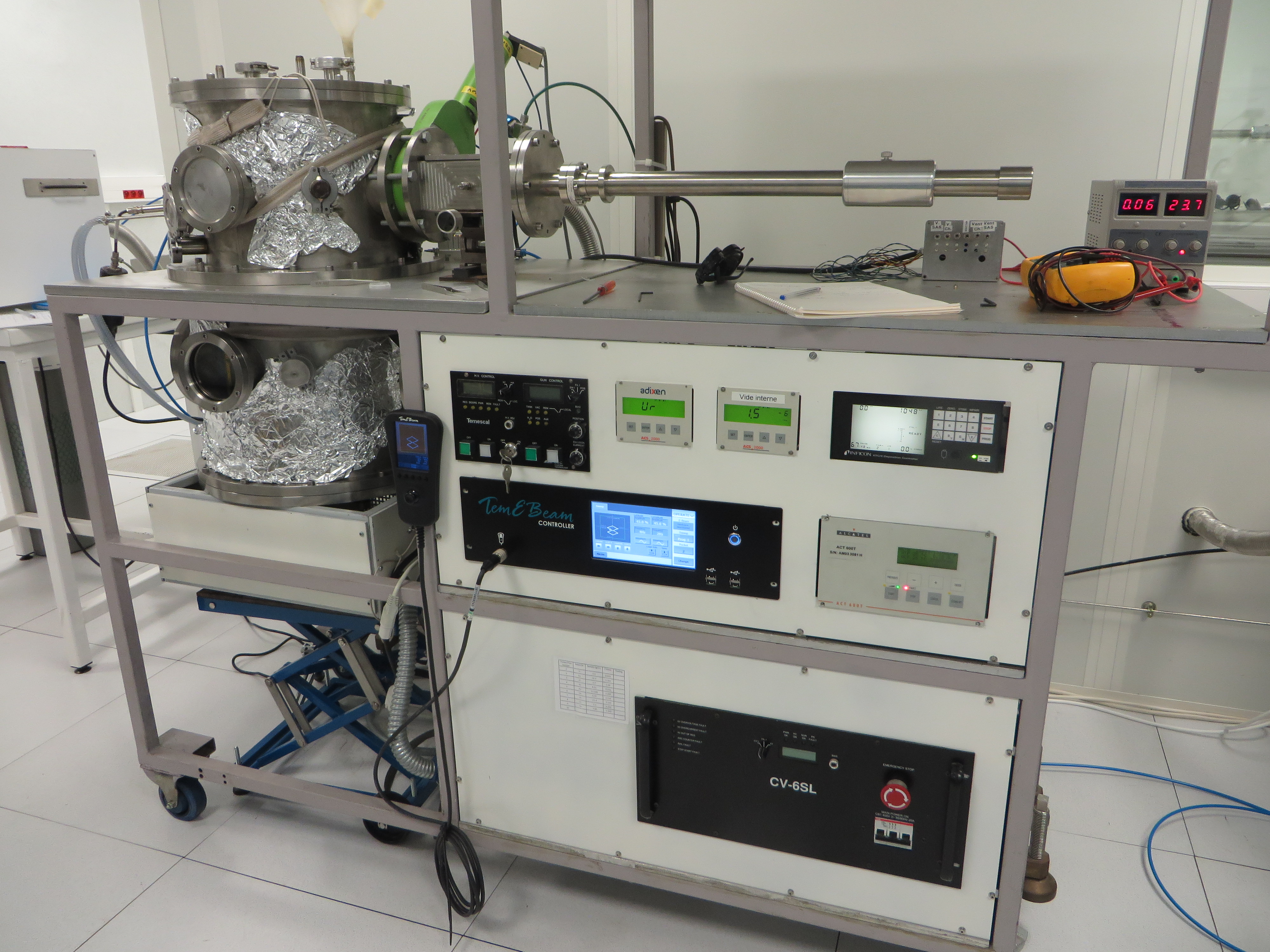
Electron gun evaporation
The electron gun evaporator is an in-house system. It is equipped with a Ferrotec gun, with 8 crucibles and a sample holder allowing to make tilted evaporation. It has been fabricated thanks to the «mechanical» and «instrumental development» design offices for the design, Mr. Perrin and Pace for the control electronics and the mechanical manufacturing for the realisation of sub-assemblies.
Materials: Ti, Cr, Au, Al, Ge, Pt, Ni and Pd.
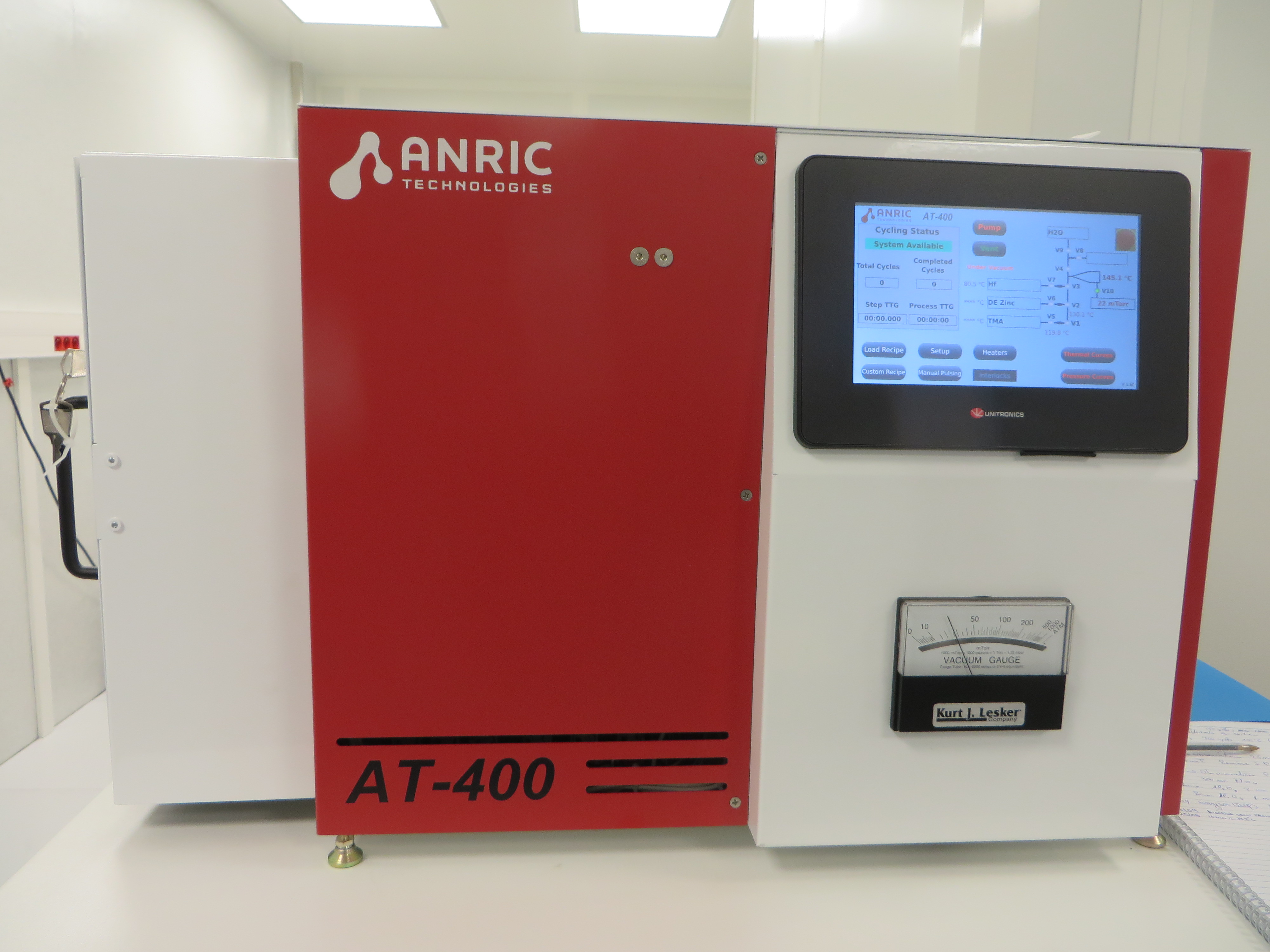
Oxyde deposition by ALD
The ALD deposition oven (Atomic Layer Deposition) is an AT400 ANRIC. It allows to deposit high-κ dielectrics, such as aluminium oxide (Al2O3) and hafnium oxide (HfO2). The precursors are H2O, with TMAl or TDMAH, under 250mTorr nitrogen, and deposited at temperatures between 50 and 200°C. Deposition on substrates up to 4″, with layer thickness from 1 to 100nm. Deposition of ZnO (from DEZn) and TiO2 (from TDMAT) also possible .
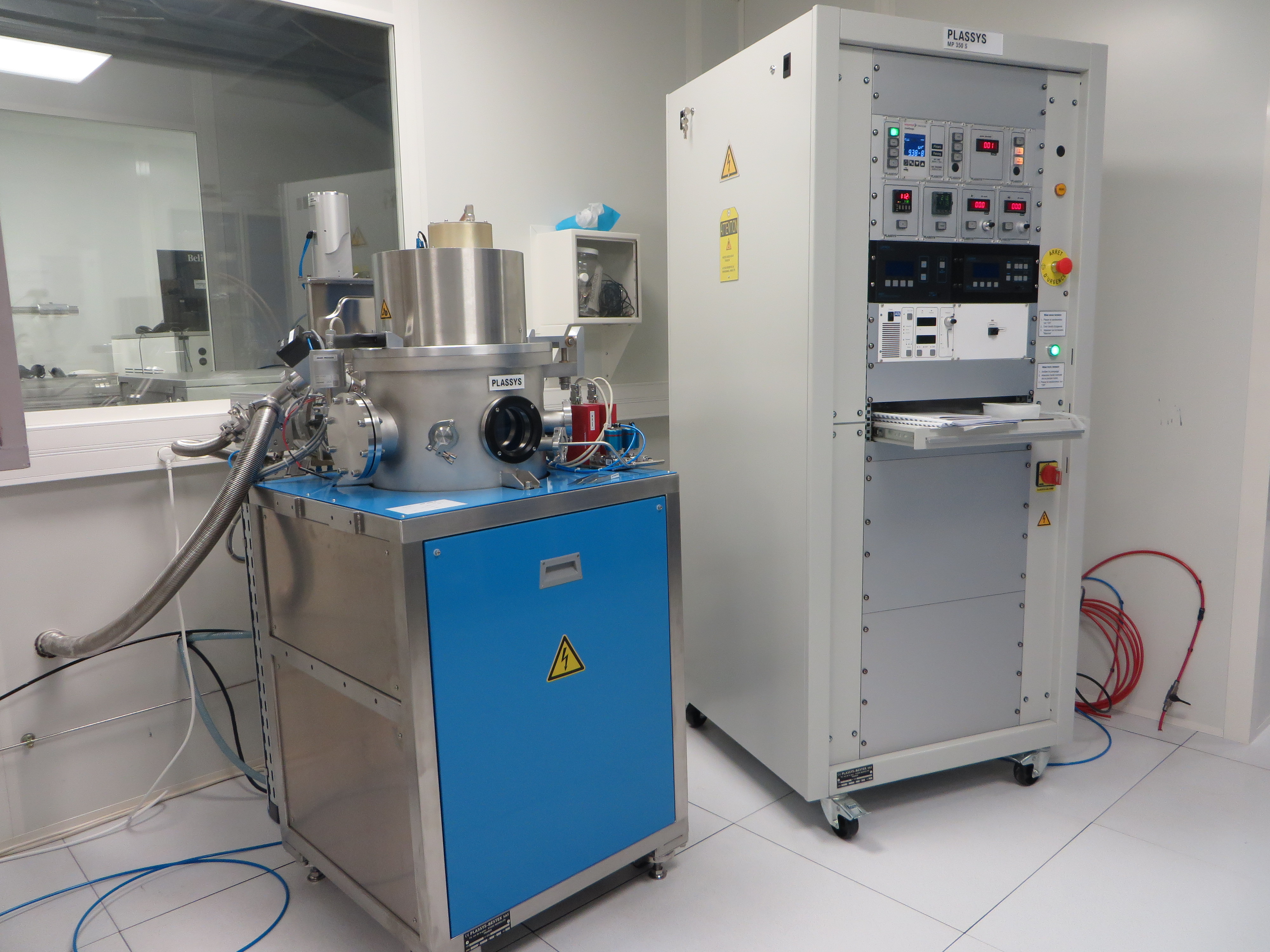
Sputtering
The sputtering is a Plassys MP350S system. It is made to deposit high quality superconductors, thanks to its high vacuum. It has 2 DC magnetron cathodes of 2’’ with an ADL 1kW source. The sample holder can rotate and be warmed up up to 600°C. A RF ion milling plasma etching with Argon is also possible.
Targets: Nb, Ta.
Growth pole
CNT oven
The CVD oven for the carbon nanotube synthesis is a home-made tubular “hot-wall” system. The gaseous precursors are Ar, H2 et CH4, operating at atmospheric pressure.
The oven also allows to make annealing under Ar/H2 up to 1000°C.
Transfer station for 2D materials
Stamper for 2D materials used for the fabrication of Van der Waals heterostructures. XYZ manual stages for the stamp, xyθ for the substrate and xyz for the microscope. Heating up to 125°C. Made by the mesoscopic physics team.
Mastering of the BN-Gr-BN heterostructures fabrication with the so-called “Columbia” method (based on suspended PPC), “modified Columbia” (based on PDMS and PPC droplet) and the so-called “Aachen” method (based on PVA and PMMA).
Characterisation pole
AFM
The atomic force microscope (AFM) is a Veeco (Bruker) Dimension Edge. Taping mode, contact mode and MFM (Magnetic Force Microscopy). It has a spatial resolution of 0.3nm in thickness and of the order of 15nm in the plane (tip bend radius). The maximum mesurable thickness is 4μm and the maps can be up to 50×50μm.
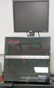
Mechanical profilometer
The mechanical profilometer is a Veeco (Bruker) Dektak 8, equipped with a tip of a bend radius of 2μm. The measurable height range is from 20nm to 1mm.
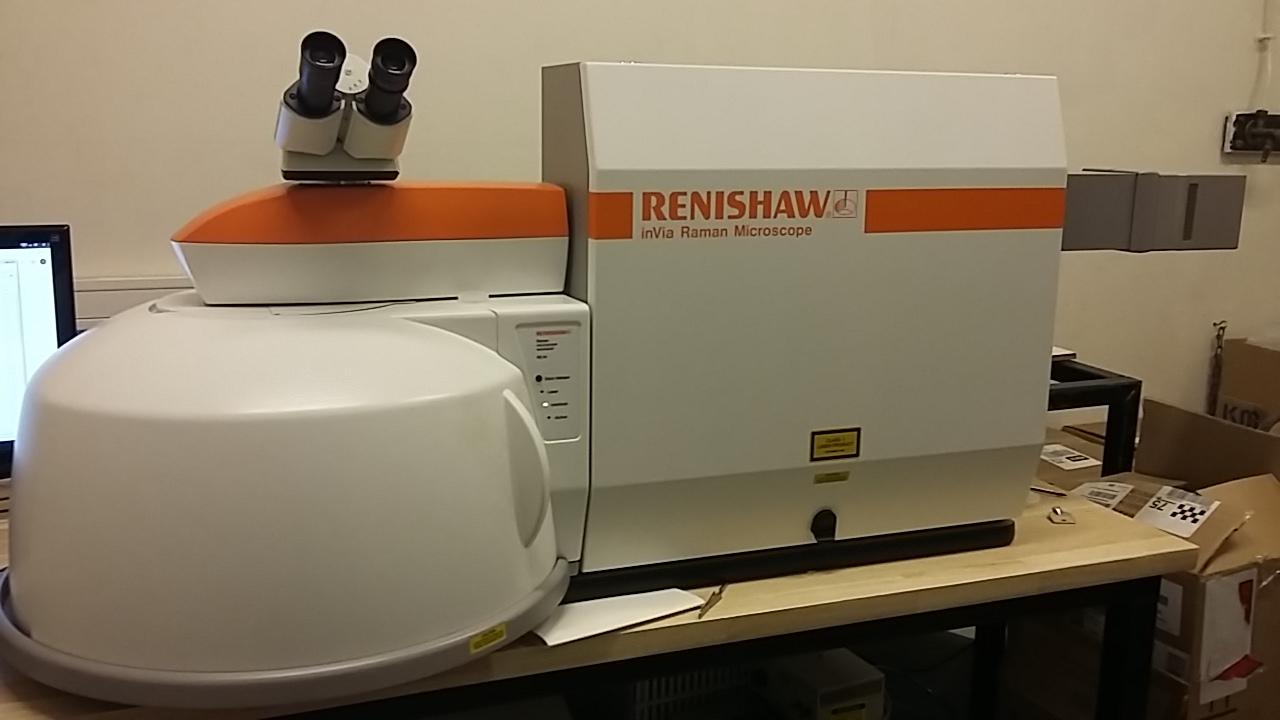
Raman spectrometer
The Raman spectrometer is a Renishaw InVia Reflex, equipped with 2 lasers, one in the green at 532nm and one in the red at 633nm. With 5x, 20x, 50x and 100x objectives, it allows to acquire spatial maps with the spatial resolution limit (400nm). Its spectral resolution is of few cm-1. Its Edge filters allow to make measurements down to 50cm-1 with the green laser and down to 100cm-1 with the red one. It is also equipped with a Notch filter to acquire Stokes/anti-Stokes measurements with the green laser (+200cm-1/-400cm-1).
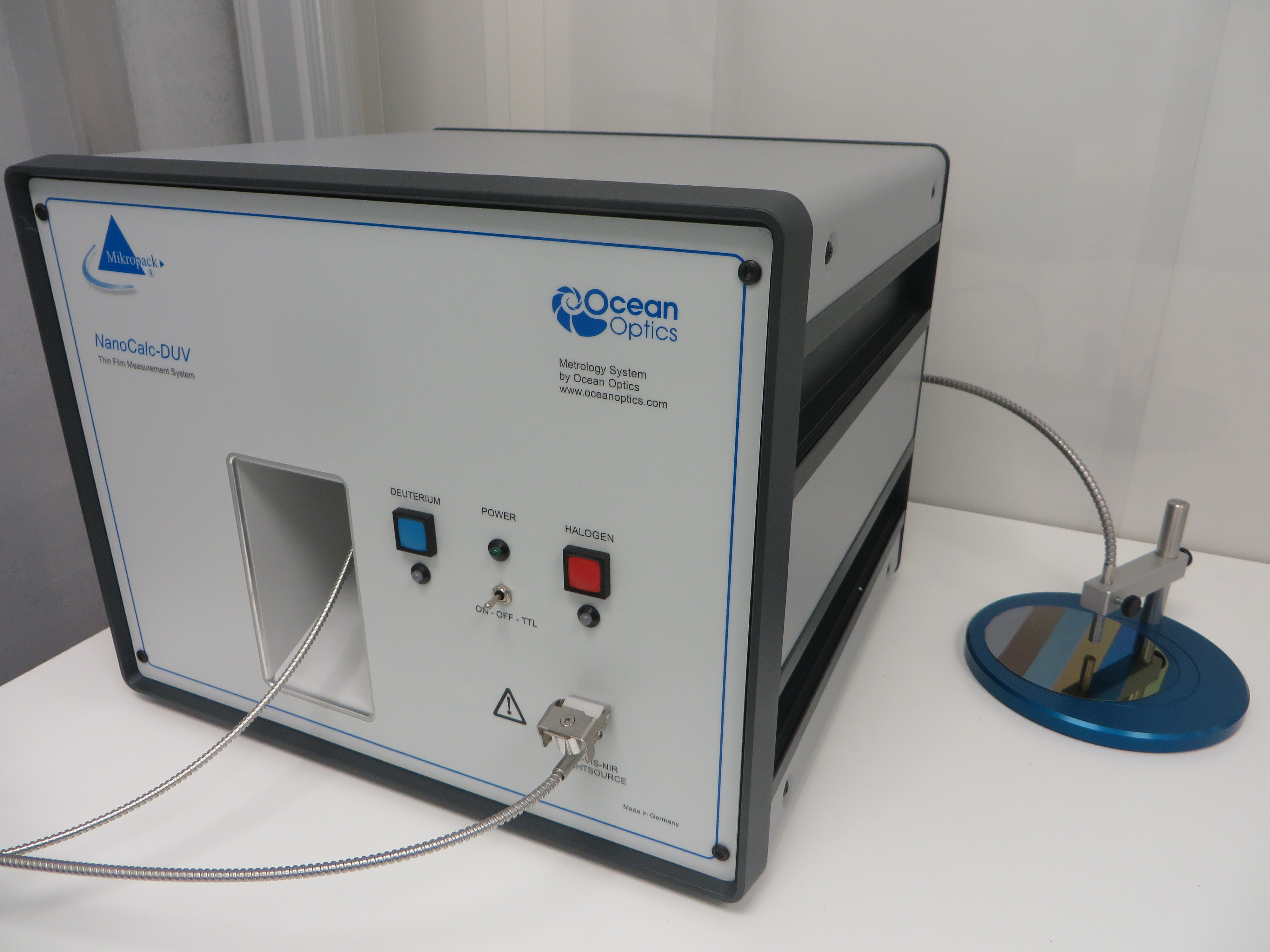
Reflectometer
The reflectometer is a NanoCalc-DUV Ocean Optics system, allowing to measure oxyde thickness from 10nm to 70μm with a precision of few nm. It is equipped with a halogen source and a deuterium one, covering the 200nm-1100nm range.
Back-end pole
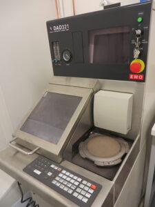
Diamond saw
The Disco DAD321 diamond saw allows to dice Si, quartz and sapphire substrates up to 6″. The cutting band width is around 100μm.
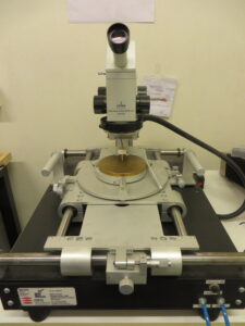
Scriber
The scriber is a MR-100 OEG.