


Light sources will play a key role in emerging quantum technologies, including single-photon sources in crystalline materials. In this context, by exciting a two-dimensional material with an electron microscope beam, researchers have uncovered promising new sources for the realisation of large-scale quantum devices with homogeneous spectral properties and controlled spatial arrangement.
Light particles –or photons– allow quantum information to be conveyed at a distance with a high fidelity. For this reason, single photon sources are considered an important building block for quantum technologies. The integration of such sources in a solid-state matrix allows the realisation of large-scale devices. In this context, new two-dimensional materials (like graphene) have been considered very promising for some years. Among them is hexagonal boron nitride. It is a transparent lamellar material from which it is possible to create miniaturised devices controlled at the ultimate scale of a few atomic layers. It is known to contain ” colour centres “, crystal defects that can emit single photons. However, these colour centres have the disadvantage of having random emission wavelengths and positions in the crystal. These characteristics limit their use for quantum information, which requires sources with controlled and reproducible properties.
Engineers from the Laboratoire de physique de l’ENS (LPENS, CNRS/ENS Paris/Sorbonne University/Université de Paris) in partnership with the NIMS (Japan) have fabricated the samples allowing the Groupe d’étude de la matière condensée (GEMaC, CNRS/Université Versailles St-Quentin) to demonstrate the existence of a new family of colour centres in hexagonal boron nitride. These single photon sources have the advantage of all emitting at very close wavelengths, which is a rare property. In addition, these emitters are created in a localised manner, by interaction with the beam of a scanning electron microscope, which allows their position to be controlled on a submicrometre scale. The next step is to obtain a single photon source by interaction with the electron beam. This will pave the way for spatially controlled integration of single photon sources into optical devices such as waveguides or optical microcavities: a new approach for the realisation of integrated ‘quantum chips’ based on indistinguishable single photons.
This work has been published in Nature Communications and highlighted on CNRS INP: https://inp.cnrs.fr/fr/cnrsinfo/des-sources-de-lumiere-quantique-positionnees-de-facon-controlee-dans-un-materiau-2d

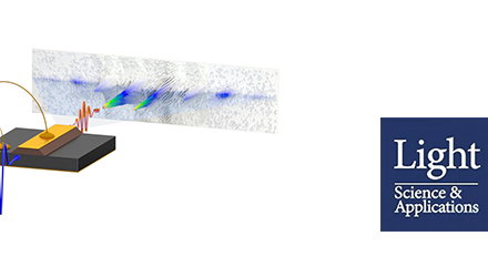
Left: electron microscope image of a 60 nanometre thick hexagonal boron nitride flake. The circles indicate the positions chosen to activate quantum emitters.
Right: confocal mapping of the luminescence of the flake. The yellow areas indicate light emission from the colour centres. There are about 15 emitters per electron beam impact.
More :
Position-controlled quantum emitters with reproducible emission wavelength in hexagonal boron nitride. C. Fournier, A. Plaud, S. Roux, A. Pierret, M. Rosticher, K. Watanabe, T. Taniguchi, S. Buil, X. Quelin, J. Barjon, J.-P. Hermier et A. Delteil, Nature Communications
https://doi.org/10.1038/s41467-021-24019-6
Author affiliation :
Laboratoire de physique de L’École normale supérieure (LPENS, ENS Paris/CNRS/Sorbonne Université/Université de Paris)
Corresponding author : Aurélie Pierret Michael Rosticher
Communication contact : L’équipe de communication